Applied Physics- Electronic Devices & Materials

Applied Physics- Electronic Devices & Materials

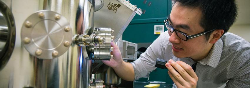
The program focuses on the fundamental physics and device applications of advanced electronic and optoelectronic devices, MEMS, microfluidic and biomedical devices, as well as on the science and engineering of new materials and device structures at the micro-, nano-, and atomic scales. This program is highly interdisciplinary and explores broader applications in revolutionizing electronics, optoelectronics, and medicine.

Research areas:

  • Compound semiconductor epitaxial growth and heterostructure devices
  • Hybrid and monolithic heterogeneous integration of high-performance materials to Silicon
  • Advanced CMOS devices and circuits
  • Spin-related devices
  • Advanced optical MEMS, bio-MEMS and RF MEMS
  • Organic and inorganic semiconductor nanostructures
  • Micro- and nano-fabrication
  • Advanced technologies for nanoscale imaging and metrology
  • Advanced nano-sensors (photo, force, temperature, chemical, biological)
  • Electro-neural interfaces and neural probing
  • Photovoltaics, thermoelectrics, and renewable energy
  • Fusion energy materials and engineering
  • Structure-Property correlation in novel materials and devices
  • Nanolasers and nanophotonics
  • Artificial photosynthesis and CO2 reduction
  • Printed and flexible electronics
  • Microfluidic and nanofluidic devices
  • Bioelectronic and biophotonic devices
  • Medical devices

Application areas:

  • Wireless communications and other high-frequency systems
  • High-speed optical communications and microwave photonics
  • Information storage and manipulation
  • Digital VLSI systems
  • Renewable and clean energy harvesting devices and systems
  • Biological and chemical sensing
  • Reliable human-machine interfaces and prosthetic devices
  • Drug delivery and medicines
  • Bioinspired devices and systems
  • Cell-based and molecular-based assays for medicine

Sample Program Description:

The synthesis of novel material structures, such as epitaxial III-V compound semiconductor materials, is performed using our molecular beam epitaxy (MBE) and organometallic vapor phase epitaxy (OMVPE) facilities. Charles Tu is involved with the epitaxial layer growth of heterojunctions and nanostructures of binary, ternary, and quaternary III-V compound semiconducting alloys. This includes some exciting work on dilute nitrides (~1% nitrogen in III-V compounds) for intermediate band solar cells and for nanowire solar cells.

The rational growth of nano-materials and structures including semiconductor nanowires and (radial, axial, and branched) heterostructures using CVD, MOCVD, solution growth, and by nanofabrication, have opened up interdisciplinary research in the areas of materials science, chemistry, solid state physics, and nanofabrication. The exciting examples include ultra-high sensitivity nanowire photodetectors, zero subthreshold slope nanowire NEMS-FET, high-efficiency nano-tree photovoltaic cells for hydrogen production from sea water, as well as high-density nanowire artificial neurosensory retina arrays. In addition, Tse Nga Tina Ng is developing novel device fabrication techniques for flexible electronics, to enable new form factor and functionalities through scalable additive manufacturing.

With continuous reduction of device dimensions for faster operation, reduced power, and increased density and functionality, structure-property correlation at nano to atomic scales becomes vital to understand the influence of material imperfections on their device performance. As such, materials characterization is carried out by a range of techniques within the department. It is used to determine the microstructural, electrical, electro-optic, galvanomagnetic and optical properties of bulk layers, heterojunctions, quantum wells, superlattices, and other nanostructures. In-situ microscopy is used to gauge atomic scale reactions and processes in advanced semiconductor devices. S. S. Lau, Shadi Dayeh and their associates are working on electronic materials science and technology, including hetero-materials integration and flexible electronics.

Optoelectronics research at UCSD includes the study of optoelectronic and high-speed heterostructure devices and systems. Nano- and micro-scale engineered materials and devices (e.g., Nanolasers and Nanophotonics integration into photonic lightwave circuits (PLC)) for CMOS compatible manufacturing and integration with electronics. William Chang, Shayan Mookherjea, Shaya Fainman and Paul Yu are primarily interested in optical guided wave devices, quantum well and superlattice guided wave switches, modulators, and high power detectors and sensors, for microwave signal transmission in fibers and via free space.

For electronic circuits, there is a major research effort in the area of high-frequency transistors and ICs. The objectives of this program include exploring a variety of semiconductor materials for microwave and mm-wave transistor operation, as well as for ultralow power; determining limits of device scaling and performance; device modeling; developing advanced transistor circuits; and the integration of electronic and photonic devices. Material systems currently being investigated for transistors include GaN, silicon-on-insulator,  and graphene.  Compound semiconductors GaSb and GaInAs are also being investigated to fabricate tunneling MOSFETs which promise to dramatically reduce power dissipation in digital circuits. This research area is currently being pursued by Peter Asbeck and Yuan Taur.

The scaling of IC technology to 10 nm with a supply voltage below 0.5 V demands paradigm shifts in both the material and device architecture. Low dimensionality materials are promising candidates for nanometer scale transistors because of their near atomic thickness and diameters. To contain the off state power, a turnoff slope steeper than the conventional thermal limit is required. Yuan Taur’s group conducts in depth analysis and comprehensive modeling of tunnel FETs as well as MOSFETs made in 2D and 1D semiconductors. The research outcome on the switching delay and power as a function of power supply voltage gives key insights to the direction of future IC technology post 10 nm node below 0.5 V supply voltage.

Another area of high-frequency research is RF MEMS (Radio Frequency Micro-Electro-Mechanical Systems) with a goal of creating miniature switches and varactors with very low loss up to 100 GHz. These devices are used in reconfigurable radios front-end circuits such as tunable antennas, tunable filters, tunable power amplifiers. RF MEMS devices are built using surface micromachining techniques on silicon and glass wafers, and can therefore be fabricated on a very large scale at low cost. They have the potential to change the way we build wideband radios, and with applications in defense and commercial communication systems (3G, 4G, etc.). This research is currently pursued by Gabriel Rebeiz.

The biomedical device research includes applications of microfluidic, electronic, photonic, and acoustic technologies to produce lab-on-a-chip devices for medical research and point-of-care clinics. We apply engineering methods to develop unique tools to accelerate discoveries in medicine, to translate medical discoveries to clinical applications for improved patient outcomes, and to significantly reduce the cost of health care. Examples of projects include (a) lab-on-a-chip flow cytometers for cell analysis for immunology, cancer clinics, infectious diseases, and food safety, (b) whole blood analysis devices for cancer patients undergoing chemotherapy and kidney disease patients receiving peritoneal dialysis, (c) microfluidic devices for detection and isolation of circulating tumor cells (CTCs) for cancer prognosis, (d) microfluidic devices for on-chip micro-RNA detection and profiling for early cancer detection, (e) biomedical devices for human microbial studies, (f) nanoparticle synthesis and in vivo interaction of nano-drug delivery devices and imaging contrast agents with ultrasound, and (g) Optofluidics integrating opto-electro-fluidic devices into systems at the micro and nanometer scales for in vivo point of care medical diagnostics. The research is currently pursued by Yuhwa Lo, Shadi Dayeh, Sadik Esener, Zhaowei Liu, Shaya Fainman, Drew Hall, and Tse Nga Tina Ng.


Faculty

Emeritus Faculty